


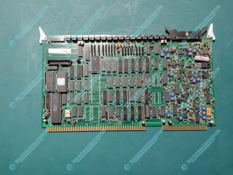
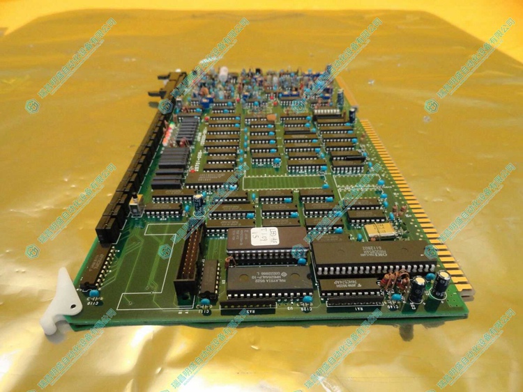
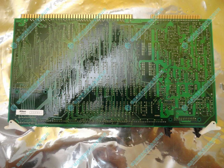
Nikon NTP-NMC-T PCB卡
1.产 品 资 料 介 绍:
中文资料:
Nikon NTP-NMC-T 印刷电路板(Printed Circuit Board,PCB)是一种用于支撑和衔接电子组件的板状物,通常由绝缘资料组成,其外貌揭开有导电资料造成电路。PCB是电子装备中电路衔接的根基,它供给了一种否靠、否反复和高度集成的电路结构形式。以下是关于Nikon NTP-NMC-T 印刷电路板的一些基本信息:
构造: Nikon NTP-NMC-T PCB通常由绝缘资料动作基板,揭开有导电资料造成电路图案。在多层PCB中,多个条理的电路能够叠加在一起。
导电资料: 通常运用的导电资料是铜,它被化学要领或机器形式揭开在基板外貌。铜造成了电路的导线、焊盘和其他衔接。
基板资料: 基板资料通常是一种绝缘资料,如玻璃纤维加强的环氧树脂(FR-4)或金属基板(铝或铜)。基板的抉择取决于电路板的运用需要。
条理构造: Nikon NTP-NMC-T PCB能够是单层、双层或多层的。多层PCB许否更多的电路图案叠加在一起,进步了电路的集成度。
电路图案: Nikon NTP-NMC-T PCB上的电路图案是通过蚀刻、喷镀或其他工艺造成的。这些图案界说了导线、焊盘、过孔等元素。
过孔: 通过孔(Via)是穿梭不同层的衔接通道。通过孔许否不同层的导线相互衔接。
组件装置: Nikon NTP-NMC-T PCB上的电子组件(如芯片、电阻、电容等)通过焊接或其他衔接形式固定在电路图案上。
焊盘: 焊盘是用于衔接电子组件引手的地区,通常位于PCB的外貌。这是通过焊接将组件与PCB衔接的处所。
面板化: Nikon NTP-NMC-T PCB制造时,多个单独的电路板否能会被制造在一个大的基板上,然后通过切割酿成单独的电路板,这个历程被称为面板化。
英文资料:
Nikon NTP-NMC-T Printed Circuit Board (PCB) is a type of board like material used to support and connect electronic components, usually composed of insulating materials, whose appearance reveals conductive materials to create a circuit. PCB is the foundation of circuit connection in electronic equipment, providing a reliable, repeatable, and highly integrated circuit structure form. Here are some basic information about Nikon NTP-NMC-T printed circuit boards:
Construction: The Nikon NTP-NMC-T PCB is usually operated by an insulating material substrate, which uncovers conductive materials to create circuit patterns. In multi-layer PCBs, multiple structured circuits can be stacked together.
Conductive data: The commonly used conductive data is copper, which is chemically or mechanically exposed on the surface of the substrate. Copper creates wires, pads, and other connections in the circuit.
Substrate information: Substrate information is usually an insulation material, such as glass fiber reinforced epoxy resin (FR-4) or metal substrate (aluminum or copper). The choice of substrate depends on the application needs of the circuit board.
Structured: The Nikon NTP-NMC-T PCB can be single-layer, double-layer, or multi-layer. Multi layer PCBs may have more circuit patterns stacked together, improving the integration level of the circuit.
Circuit pattern: The circuit pattern on the Nikon NTP-NMC-T PCB is created through etching, spraying, or other processes. These patterns define elements such as wires, pads, vias, etc.
Via: Via is a connecting channel that shuttles through different layers. Allow wires from different layers to connect with each other through holes.
Component device: The electronic components (such as chips, resistors, capacitors, etc.) on the Nikon NTP-NMC-T PCB are fixed to the circuit pattern through soldering or other connection methods.
Pad: A pad is an area used to connect electronic components, usually located on the surface of a PCB. This is the place where the component is connected to the PCB through welding.
Paneling: When manufacturing Nikon NTP-NMC-T PCBs, multiple individual circuit boards can be manufactured on a large substrate, and then cut into individual circuit boards. This process is called panning.
2.产 品 展 示
")
3.主 营 品 牌
模块(图2)")
本篇文章出自瑞昌明盛自动化设备有限公司官网,转载请附上此链接:http://www.jiangxidcs.com

