


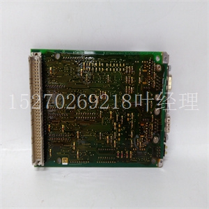
GFD212A 3BHE020356R0101 3BHE020357P201控制卡件
MC2芯片LCSR(本地控制/状态寄存器)。安装跳线时,位值读取为零,拆除跳线时,读取为一。(出厂配置)VMEbus+5V STBY J20 1 2 5 6 J20 1 5 6 J21 2备用电源禁用车载电池5 6(仅用于存储)1 2 3 J21 8Mbit EPROM 1 2 3(出厂配置:J21 4Mbit EPROM 2-12计算机组文献中心网站硬件准备2在出厂安装MVME162Bug固件后,用户可定义四个跳线(引脚1-2、3-4、5-6、7-8)。如果移除了MVME162Bug固件,则用户可以定义七个跳线(引脚1-2、3-4、5-6、7-8、11-12、13-14、15-16)。注:引脚9-10(GPI3)用于选择闪存映射(已安装跳线)或EPROM内存映射(已移除跳线)。它们不是用户可定义的。有关更多信息,请参阅第3章。在大多数情况下,控制器出厂时J22设置为全零(跳线安装在所有引脚上)。然而,在并没有VMEbus选项的控制器板上,并没有跳线安装在引脚9-10之间。J22 15 GPI7 GPI6 GPI5 GPI1 GPI4 GPI3 GPI2 1 2 GPI0 16闪存已选择(工厂配置,无VMEbus型号除外)用户可定义用户可定义参考162BUG手册用户可定义In=闪存;Out=EPROM参考162BUG手册参考162BUB手册162BUG已安装用户可定义用户可定义;输出=EPROM用户可定义用户可定义安装的用户代码9 10系统控制器选择标题(J1)http://www.mcg.mot.com/literature2-13 2 MPU热调节集管(J23)该集管保留供将来使用。默认出厂配置为未安装跳线。IP总线时钟标题(J24)此标题选择IP总线时钟的速度。IP总线时钟速度可以是8MHz(在MVME162-4xx和-5xx板上)或32MHz(仅在MVME162-5xx板)。默认出厂配置是在J24上安装跳线,引脚1和2表示8MHz时钟。如果跳线安装在J24上的引脚2和3之间,IP总线时钟与MC68040总线时钟(32MHz)相同,因此允许IP模块使用32MHz MPU运行。无论设置为8MHz还是32MHz,所有IP端口都以相同的速度运行!警告IP32 CSR位(IP2芯片,偏移$1D处的寄存器,位0)必须设置为与跳线设置相对应。8MHz时清除(0),32MHz时设置(1)。如果跳线和位配置不相同,则电路板可能无法正常运行。1 2(出厂配置)J23未使用3 2 1 3 2 1(出厂设置)J24 8MHz IP总线时钟J24 32MHz IP总线时钟(来自MPU总线时钟)2-14计算机组文献中心网站硬件准备2注意:某些版本的控制器(组件号为01-W3960Bxxx的控制器)可能在8MHz位置使用J24工厂硬接线,隐藏在IP模块下面。将出厂设置更改为32MHz设置需要移除引脚1和2之间的缝钉,并在引脚2和3之间安装跳线。IP总线选通头(J25)一些IP总线实现使用选通*信号(引脚46)作为来自IP2芯片的IP模块的输入。其他IP接口要求断开选通。通过在J25引脚1和2之间安装跳线,可编程频率源连接到IP总线上的Strobe*信号。有关更多信息,请参阅《MVME162FX嵌入式控制器程序员参考指南》中的IP2芯片编程模型。如果从J25中移除跳线,则选通线路可用于IP模块之间的边带类型的消息传递。
MC2 chip LCSR (Local Control/Status Register). The bit values are read as a zero when the jumper is installed and as a one when the jumper is removed. (Factory configuration) VMEbus +5V STBY J20 1 2 5 6 J20 1 2 5 6 J20 1 2 Backup Power Disabled Onboard Battery 5 6 (For storage only) 1 2 3 J21 8Mbit EPROM 1 2 3 (Factory configuration) J21 4Mbit EPROM 2-12 Computer Group Literature Center Web Site Hardware Preparation 2 With the factory installed MVME162Bug firmware in place, four jumpers are user-definable (pins 1-2, 3-4, 5-6, 7-8). If the MVME162Bug firmware is removed, seven jumpers are user-definable (pins 1-2, 3- 4, 5-6, 7-8, 11- 12, 13-14, 15-16). Note Pins 9-10 (GPI3) are reserved to select either the flash memory map (jumper installed) or the EPROM memory map (jumper removed). They are not user-definable. Refer to Chapter 3 for additional information. In most cases, the controller is shipped from the factory with J22 set to all zeros (jumpers installed on all pins). On controller boards built with the no-VMEbus option, however, there is no jumper is installed across pins 9- 10. J22 15 GPI7 GPI6 GPI5 GPI1 GPI4 GPI3 GPI2 1 2 GPI0 16 Flash Selected (factory configuration except on no-VMEbus models) User-definable User-definable User-definable Refer to 162BUG Manual User-definable In = Flash; Out=EPROM Refer to 162BUG Manual Refer to 162BUG Manual 162Bug Installed User-definable User-definable User-definable User-definable User-definable In = Flash; Out=EPROM User-definable User-definable User Code Installed 9 10 System Controller Select Header (J1) http://www.mcg.mot.com/literature 2-13 2 MPU Thermal Regulation Header (J23) This header is reserved for future use. Default factory configuration is with no jumper installed. IP Bus Clock Header (J24) This header selects the speed of the IP bus clock. The IP bus clock speed may be 8MHz (on both MVME162-4xx and -5xx boards) or 32MHz (on MVME162-5xx boards only). The default factory configuration is with a jumper installed on J24, pins 1 and 2 denoting an 8MHz clock. If the jumper is installed on J24, between pins 2 and 3, the IP bus clock is the same as the MC68040 bus clock (32MHz), thus allowing the IP module to run with a 32MHz MPU. Whether the setting is 8MHz or 32MHz, all IP ports operate at the same speed. ! Caution The IP32 CSR bit (IP2 chip, register at offset $1D, bit 0) must be set to correspond to the jumper setting. This is cleared (0) for 8MHz, or set (1) for 32MHz. If the jumper and the bit are not configured the same, the board may not run properly. 1 2 (Factory configuration) J23 Not used 3 2 1 3 2 1 (Factory configuration) J24 8MHz IP Bus Clock J24 32MHz IP Bus Clock (from MPU Bus Clock) 2-14 Computer Group Literature Center Web Site Hardware Preparation 2 Note Some versions of the controller (those identified with assembly number 01-W3960Bxxx) may have J24 factoryhardwired in the 8MHz position with a staple between J2 pins 1 and 2, hidden beneath an IP module. Changing the factory setting to the 32MHz setting requires removal of the staple between pins 1 and 2, and installation of a jumper between pins 2 and 3. IP Bus Strobe Select Header (J25) Some IP bus implementations make use of the Strobe∗ signal (pin 46) as an input to the IP modules from the IP2 chip. Other IP interfaces require that the strobe be disconnected. With a jumper installed between J25 pins 1 and 2, a programmable frequency source is connected to the Strobe∗ signal on the IP bus. Refer to the IP2 chip programming model in the MVME162FX Embedded Controller Programmer’s Reference Guide for additional information. If the jumper is removed from J25, the strobe line is available for a sideband type of messaging between IP modules.
")
")
")
")

