


HCS02.1E-W0012-A03-NNNN工控自动化卡件
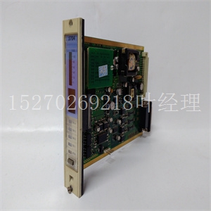
嵌入式控制器。它包含产品的一般概述,以及硬件功能列表和详细的功能描述。控制器的前面板开关和指示灯包含在功能说明中。此外,本章末尾提供了一节内存映射,以使您熟悉控制器的内存地址和访问的相应设备。《MVME162FX嵌入式控制器程序员参考指南》涵盖了ASIC中的所有控制器可编程寄存器。概述MVME162FX嵌入式控制器基于MC68040或MC68LC040微处理器。各种版本的控制器具有4MB、8MB或16MB的无保护DRAM、8KB的SRAM(带备用电池)、时钟(带备用)、以太网收发器接口、带EIA-232-D或EIA-530或EIA-485/422接口的两个串行端口、六个计时定时器、看门狗定时器、PROM插槽、1MB闪存(一个闪存设备)、四个带DMA的工业包(IP)接口、,带有DMA的SCSI总线接口、VMEbus控制器和512 KB的SRAM(带备用电池)。控制器的I/O连接到VMEbus P2连接器。主板通过P2过渡板和电缆连接到过渡板。MVME162FX嵌入式控制器支持以下转换板:❏ MVME712-12 1-2计算机组文献中心网站板级硬件描述1❏ 最小值712-13❏ 最小值712m❏ MVME712A型❏ 上午712点❏ MVME712B(本手册中称为MVME712x,除非另有规定)MVME712 x转接板为I/O设备提供配置头和行业标准连接器。控制器的串行端口I/O连接也通过两个DB25前面板I/O连接器实现。MVME712系列转接板设计用于支持MVME167板,但可通过采取一些特殊预防措施在MVME162FX嵌入式控制器上使用(有关更多信息,请参阅本章中的串行通信接口部分)。这些转换板为I/O设备提供配置头、串行端口驱动程序和行业标准连接器。VMEbus接口由称为VMEchip2的ASIC提供。VMEchip2包括两个滴答计时器、一个看门狗计时器、用于主接口和从接口的可编程映射解码器、一个VMEbus到/来自本地总线DMA控制器、一个VM总线到/来自非DMA编程访问接口、一个VMSbus中断器、一个VDEbus系统控制器、一种VMEbus中断处理器和一个VME总线请求器。处理器到VMEbus的传输可以是D8、D16或D32。然而,到VMEbus的VMEchip2 DMA传输可以是D16、D32、D16/BLT、D32/BLT或D64/MBLT。MC2芯片ASIC提供四个时钟定时器、LAN芯片接口、SCSI芯片、串行端口芯片、BBRAM、DRAM和/或SRAM夹层板的可编程接口以及闪存写入启用信号。工业包接口控制器(IP2芯片)ASIC提供控制和状态信息,包括可插入MVME162FX主模块的最多四个单尺寸工业包(IP)或最多两个双尺寸IP的DMA控制。介绍http://www.mcg.mot.com/literature1-3 1规范要求这些板的设计符合以下规范的要求:❏ VMEbus规范(IEEE 1014-87)❏ EIA-232-D串行接口规范,EIA❏ SCSI规范,ANSI❏ 行业包装规格,GreenSpring功能❏ 32 MHz、32位MC68040微处理器或25 MHz、32比特MC68040/MC68LC040微处理器❏ 4MB、8MB或16MB共享DRAM(无保护)❏ 512KB SRAM(带备用电池)❏ 一个JEDEC标准32针PLCC EPROM插座❏ 一个Intel 28F008SA 1M x 8闪存设备(总共1MB闪存)❏ 8K x 8非易失性RAM和时钟(带备用电池)❏ 四个32位定时定时器(在MC2芯片ASIC中),用于周期性中断❏ 用于周期性中断的两个32位时钟定时器(在VMEchip2 ASIC中)❏ 看门狗计时器❏ 八个软件中断(适用于具有VMEchip2的MVME162FX版本)1-4计算机组文献中心网站板级硬件描述
Embedded Controller. It contains a general overview of the product along with a hardware features list and a detailed functional description. The controller’s front panel switches and indicators are included in the functional description. Additionally, a section on memory maps is provided at the end of this chapter to familiarize you with the controller’s memory addresses and the corresponding devices accessed. All of the controller’s programmable registers that reside in ASICs are covered in the MVME162FX Embedded Controller Programmer’s Reference Guide. Overview The MVME162FX Embedded Controller is based on the MC68040 or MC68LC040 microprocessor. Various versions of the controller have 4MB, 8MB, or 16MB of unprotected DRAM, 8KB of SRAM (with battery backup), a time of day clock (with battery backup), an Ethernet transceiver interface, two serial ports with an EIA-232-D or EIA-530 or EIA-485/422 interface, six tick timers, a watchdog timer, a PROM socket, 1MB flash memory (one flash device), four Industry Pack (IP) interfaces with DMA, a SCSI bus interface with DMA, a VMEbus controller, and 512 KB of SRAM (with battery backup). The controller’s I/O is connected to the VMEbus P2 connector. The main board is connected through a P2 transition board and cables to the transition boards. The MVME162FX Embedded Controller supports the following transition boards: ❏ MVME712-12 1-2 Computer Group Literature Center Web Site Board Level Hardware Description 1 ❏ MVME712-13 ❏ MVME712M ❏ MVME712A ❏ MVME712AM ❏ MVME712B (referred to in this manual as MVME712x, unless separately specified) The MVME712x transition boards provide configuration headers and industry-standard connectors for I/O devices. The controller’s I/O connection for the serial ports is also implemented with two DB25 front panel I/O connectors. The MVME712 series transition boards were designed to support the MVME167 boards, but can be used on the MVME162FX Embedded Controller by taking some special precautions (refer to the Serial Communications Interface section in this chapter for additional information). These transition boards provide configuration headers, serial port drivers and industry-standard connectors for the I/O devices. The VMEbus interface is provided by an ASIC called the VMEchip2. The VMEchip2 includes two tick timers, a watchdog timer, programmable map decoders for the master and slave interfaces, a VMEbus to/from the local bus DMA controller, a VMEbus to/from the local bus non-DMA programmed access interface, a VMEbus interrupter, a VMEbus system controller, a VMEbus interrupt handler, and a VMEbus requester. Processor-to-VMEbus transfers can be D8, D16, or D32. However, VMEchip2 DMA transfers to the VMEbus can be D16, D32, D16/BLT, D32/BLT, or D64/MBLT. The MC2 chip ASIC provides four tick timers, the interface to the LAN chip, a SCSI chip, a serial port chip, BBRAM, the programmable interface for the DRAM and/or SRAM mezzanine board, and a flash write enable signal. The Industry Pack Interface Controller (IP2 chip) ASIC provides control and status information, including DMA control for up to four single-size Industry Packs (IPs) or up to two double-size IPs that can be plugged into the MVME162FX main module. Introduction http://www.mcg.mot.com/literature 1-3 1 Specification Requirements These boards are designed to conform to the requirements of the following specifications: ❏ VMEbus Specification (IEEE 1014-87) ❏ EIA-232-D Serial Interface Specification, EIA ❏ SCSI Specification, ANSI ❏ Industry Pack Specification, GreenSpring Features ❏ 32 MHz, 32-bit MC68040 microprocessor or 25 MHz, 32-bit MC68040/MC68LC040 microprocessor ❏ 4MB, 8MB, or 16MB of shared DRAM (unprotected) ❏ 512KB of SRAM (with battery backup) ❏ One JEDEC standard 32-pin PLCC EPROM socket ❏ One Intel 28F008SA 1M x 8 flash memory device (1MB flash memory total) ❏ 8K x 8 non-volatile RAM and time of day clock (with battery backup) ❏ Four 32-bit tick timers (in the MC2 chip ASIC) for periodic interrupts ❏ Two 32-bit tick timers (in the VMEchip2 ASIC) for periodic interrupts ❏ Watchdog timer ❏ Eight software interrupts (for MVME162FX versions that have the VMEchip2) 1-4 Computer Group Literature Center Web Site Board Level Hardware Description
")
")
")
")

