


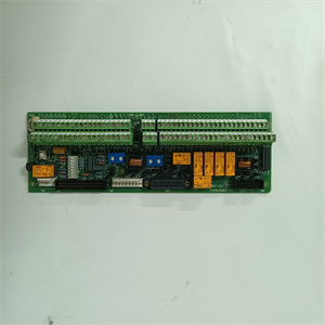
VMIVME-5521工控备件
影响设备可靠性
长时间暴露在绝对最大额定条件下可能会影响设备可靠性。规范除非另有说明参数符号测试条件最小典型值。最大单位静态漏极源极击穿电压 μ 温度系数 μ 温度系数栅极源极阈值电压μ 栅极源漏 零栅极电压漏极电流 μ 导通状态漏极电流 漏极电源接通状态电阻 接通 正向跨导 = 动态输入电容 输出电容反向转移电容总栅极电荷 = 栅极源极电荷栅极漏极电荷栅极电阻 开启延迟时间开启 身份证件 上升时间 关闭延迟时间关闭 下降时间 打开延迟时间 身份证件 上升时间 关断延迟时间 下降时间 漏极源极体二极管特性连续源极漏极二极管电流 脉冲二极管正向电流体二极管电压 体二极管反向恢复时间 μ 体二极管反向恢复电荷 反向恢复下降时间 反向恢复上升时间 。
文件编号:有关技术问题请联系:@本文件如有更改恕不另行通知。此处所述的产品和本文件受上规定的具体免责声明的约束。典型特性除非另有说明电阻输出特性与漏极电流和栅极电压栅极电荷转移特性电容导通电阻。结温 漏极到源极电压 漏极电流 到 开导通电阻漏极电压 总栅极电荷栅极到源极电流 栅极到源极电压漏极电流 漏极到源极电容 结温度标准化开导通电阻 。如有技术问题请联系:@本文件如有更改恕不另行通知。此处所述的产品和本文件受上规定的具体免责声明的约束。
Affecting equipment reliability
Prolonged exposure to absolute maximum ratings may affect equipment reliability. Unless otherwise specified in the specification, the minimum typical value of parameter symbol test condition shall be. Maximum unit static drain source breakdown voltage μ Temperature coefficient μ Temperature coefficient grid source threshold voltage μ Grid source drain zero grid voltage drain current μ On state drain current | drain power on state resistance on | forward transconductance = dynamic input capacitance output capacitance reverse transfer capacitance total grid charge = grid source charge grid drain charge grid resistance | open delay time open | ID card | rise time close delay time close down time open delay time | ID card | rise time close delay time down time Drain source diode characteristics continuous source drain diode current pulse diode forward current body diode voltage body diode reverse recovery time μ Volume diode reverse recovery Charge reverse recovery falling time Reverse recovery rising time.
Document No.: For technical problems, please contact: @ This document is subject to change without notice. The products described herein and this document are subject to the specific disclaimers set forth above. Typical characteristics Unless otherwise specified, resistance output characteristics and drain current and gate voltage gate charge transfer characteristics capacitance on resistance. Junction temperature drain to source voltage drain current to on resistance drain voltage total grid charge grid to source current grid to source voltage drain current drain to source capacitor junction temperature standardized on resistance. For technical questions, please contact: @ This document is subject to change without notice. The products described herein and this document are subject to the specific disclaimers set forth above.
")
")
")

