


")
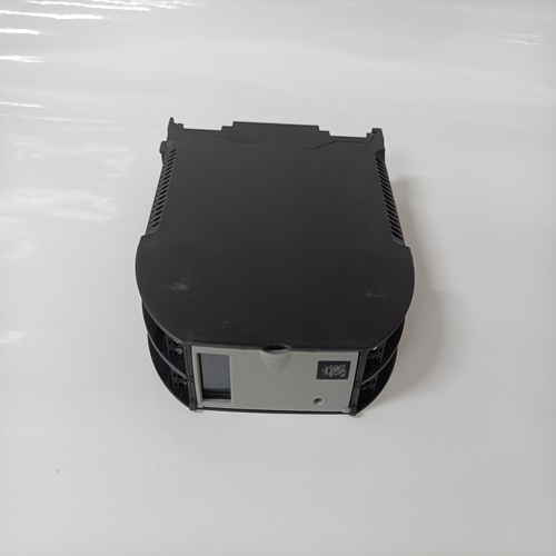
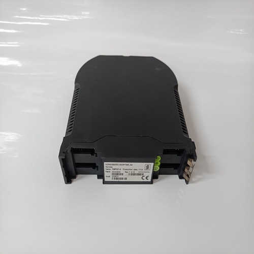
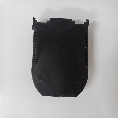
RMP201-8远程控制器
每个发电机系统中连接的单元/并联开关消除了关闭的发电机组中CT的串联电阻正在运行的发电机组的CT。
错误检测器:错误检测器电路由电压调节器组成电路、分压器、两级差分放大器 呃,还有
内部次要反馈 阿尔特。电压调整电路包括:外部电压调节变阻器VAR、电压范围调节R2和
xed电阻器R1。外部电压调整的全行程提供±10%
发电机输出电压从标称值调整。电压范围调整R2确定最大和/或最小电压
调整无功限制。电压调整电路和分压器由电阻器R5和R71组成,确定 rst微分放大器 呃。
这个 rst差分级包括晶体管Q1、Q2和Q12,电阻器R9至R18、R21、R22、R23、R83和R93、电容器C3、C23、C30和C31、铁氧体磁珠L2和L3、齐纳二极管Z1和欠频限制内的电路。低频限值(UFL)
如上所述,向晶体管Q2的基极提供参考电压
在UFL电路描述中。发电机额定运行期间频率:参考信号是恒定的,与齐纳相同
电压来自感测电路的电压,与发电机电压施加到晶体管Q1的基极。当Q1基极
电压不同于施加到基极的参考电压Q2,Q1集电极电流相对于Q2将存在差异集电极电流。
来自晶体管Q1集电极的电流由电阻器分压R9和R16
注入第二级差速器的底座
放大 类似地,来自晶体管Q2集电极的电流被电阻器R14和R15分压并注入第二级差分放大器 er晶体管Q4、电阻器R10和C3有助于防止高频振荡。第二阶段微分放大器 er振幅 es是 一级差动放大 呃。第二级差速器中包含的部件放大 er是晶体管Q3和Q4以及电阻器R24至R27
晶体管Q3的集电极电压控制相位控制电路。这个次要反馈 滤波器由电阻器R8和电容器C2组成 过滤器
从dc信号中去除任何剩余的ac。相位控制电路:T1的一个次级绕组、二极管D1、D2,D21和D22、电阻器R87和R88、电容器C20、C21和C22、电源权力 rst和第二差分级以及欠频
极限阶段。相位控制电路由二极管D5和D6组成,电阻器R28至R32和R80、电容器C20、C21和C22、齐纳二极管Z2和可编程单结晶体管(PUT)Q5。
相位控制电路是斜坡和基座控制,用于调节:功率控制器电路的相位角通过控制
它向SCR的栅极提供接通信号。指数斜坡从电压基座开始的电压提供开启选通
信号因为斜坡电压从电压基座开始基座电压振幅的小变化导致大SCR相位角的变化如图2所示。
A unit/parallel switch connected in each generator system eliminates the
series resistance of the CTs in the generator sets that are shut down from
the CTs of the generator sets that are operating.
Error detector: The error detector circuitry consists of a voltage adjust
circuit, a voltage divider, a two-stage differential ampli er, and an
internal minor feedback lter. The voltage adjust circuit consists of an
external voltage adjust rheostat VAR, a voltage range adjustment R2, and
xed resistor R1. Full travel of the external voltage adjust provides ±10%
adjustment of the generator output voltage from nominal. The voltage
range adjustment R2 establishes the maximum and/or minimum voltage
adjust limit of VAR. The voltage adjust circuit and a voltage divider
consisting of resistors R5 and R71 determine the input signal to the rst
differential ampli er.
The rst differential stage is comprised of transistors Q1, Q2, & Q12,
resistors R9 through R18, R21, R22, R23, R83, & R93, capacitors
C3, C23, C30, & C31, ferrite beads L2 & L3, Zener diode Z1, and the
circuitry within the underfrequency limit. Underfrequency limit (UFL)
provides a reference voltage to the base of transistor Q2 as described
in the UFL circuit description. During generator operation at rated
frequency the reference signal is constant and identical to the Zener
voltage. Voltage from the sensing circuit, which is proportional to the
generator voltage, is applied to the base of transistor Q1. When Q1 base
voltage is different from the reference voltage applied to the base of
Q2, there will be a difference in Q1 collector current with respect to Q2
collector current.
The current from the collector of transistor Q1 is divided by resistors
R9 and R16 and injected into the base of the second stage differential
ampli er transistor Q3. Similarly, the current from the collector of transistor Q2 is divided by resistors R14 and R15 and injected into the
second stage differential ampli er transistor Q4. Resistors R10 and
C3 help to prevent oscillations at high frequencies. The second stage
differential ampli er ampli es the output of the rst stage differential
ampli er. Components included in the second stage differential
ampli er are transistors Q3 and Q4, and resistors R24 through R27. The
collector voltage of transistor Q3 controls the phase control circuit. The
minor feedback lter consists of resistor R8 and capacitor C2. The lter
removes any remaining ac from the dc signal.Phase control circuit: One of T1s secondary windings, diodes D1, D2,
D21 & D22, resistors R87 & R88, capacitors C20, C21, & C22, supply
power to the rst and second differential stage and the underfrequency
limit stage. The phase control circuit consists of diodes D5 and D6,
resistors R28 through R32, & R80, capacitors C20, C21, & C22, Zener
diode Z2, and programmable unijunction transistor (PUT) Q5.
The phase control circuit is a ramp-and-pedestal control that regulates
the phase angle of the power controller circuit SCRs by controlling the
turn on signal it supplies to the gate of the SCRs. An exponential ramp
voltage that starts from a voltage pedestal provides the turn on gating
signal. Because the ramp voltage starts from the voltage pedestal, a
small change in the amplitude of the pedestal voltage results in a large
change in SCR phase angle as shown in Figure 2.

