


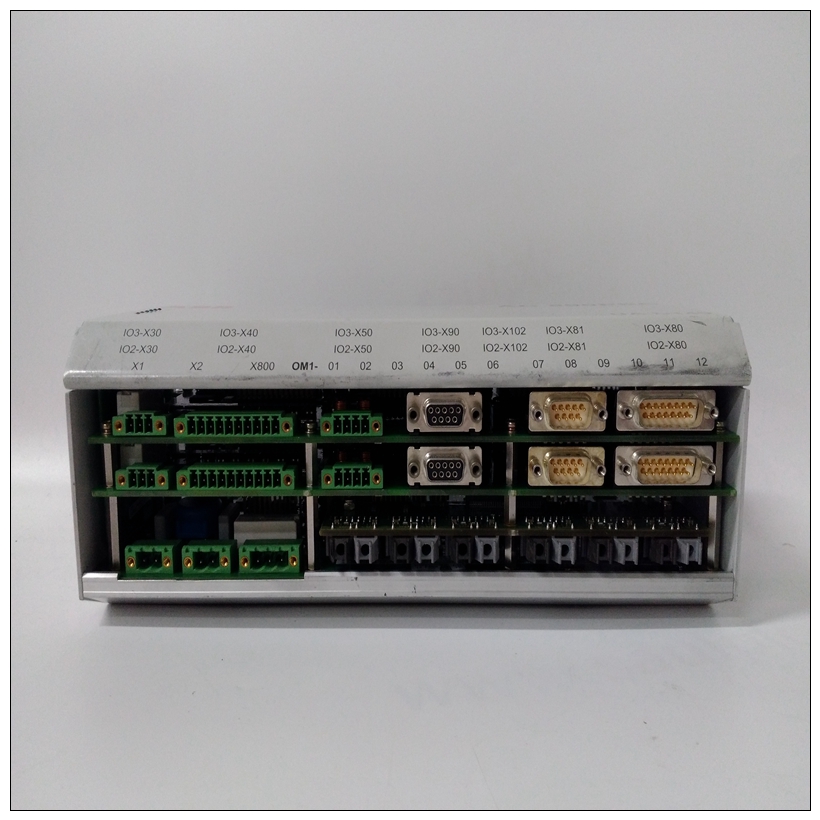
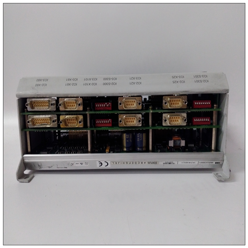
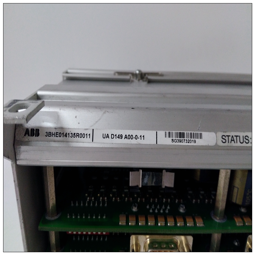

3BHE014135R0011控制模块,ABB使用过程
串行端口4传输时钟配置(J17)在同步串行通信中,您可以在上配置串行端口4MVME2603/2604使用TxC信号提供的时钟信号线收割台J17将端口4配置为驱动或接收TxC。这个出厂配置将端口4设置为接收TxC。要完成串行端口4的配置,必须设置以下内容配置标头:
❏ J16(串行端口4接收时钟配置)❏ J20(串口4发送时钟接收器缓冲控制)
")
3BHE014135R0011控制模块❏ MVME712M过渡模块上的J15或MVME761上的J3转换模块(串行端口4时钟配置)图1-9和图1-10(适用于MVME712M)以及图1-14和图1-15(对于MVME761)显示了整体跳线设置串行端口的MVME2603/2604和转换模块上需要4 DCE或DTE配置。
有关这些标头配置的更多详细信息,请参阅MVME712M过渡模块准备,第1-14页,MVME761第1-25页的过渡模块准备,或各用户的过渡模块手册(见附录D,相关文件)。串口4发送时钟接收器缓冲控制(J20)其他章节所述,串行端口4的完整配置需要在上设置以下跳线标头
MVME2603/2604或过渡模块:❏ MVME712M兼容版本的基板上的J16(串行端口4接收时钟配置)❏ J17(串行端口4传输时钟配置)❏ J20(串行端口4发送时钟接收器缓冲控制)开启MVME712M兼容版本的基板❏ MVME712M过渡模块上的J15或MVME761上的J3(串行端口4时钟配置)与发射时钟接收器缓冲器(由报头J20控制)相关联具有串行端口4。在J20上安装跳线可以启用缓冲区。正在删除跳线禁用缓冲器。出厂配置具有串行端口4缓冲区已启用。J20在MVME761兼容版本上保持开放。在MVME712M兼容版本上,J20与J17串联设置,以配置串行端口4传输时钟。如果其中一个偏离了出厂配置,那么必须另一个。
图1-9和图1-10(适用于MVME712M)以及图1-14和图1-15(对于MVME761)显示了整体跳线设置串行端口的MVME2603/2604和转换模块上需要4 DCE或DTE配置。
Serial Port 4 Transmit Clock Configuration (J17)
In synchronous serial communications, you can configure Serial Port 4 on
the MVME2603/2604 to use the clock signals provided by the TxC signal
line. Header J17 configures port 4 to either drive or receive TxC. The
factory configuration has port 4 set to receive TxC.
To complete the configuration of Serial Port 4, you must set the following
configuration headers as well:
❏ J16 (Serial Port 4 receive clock configuration)
❏ J20 (Serial Port 4 transmit clock receiver buffer control)
❏ J15 on the MVME712M transition module or J3 on the MVME761
transition module (Serial Port 4 clock configuration)
Figure 1-9 and Figure 1-10 (for the MVME712M) and Figure 1-14 and
Figure 1-15 (for the MVME761) diagram the overall jumper settings
required on the MVME2603/2604 and transition module for a Serial Port
4 DCE or DTE configuration.
For additional details on the configuration of those headers, refer to
MVME712M Transition Module Preparation on page 1-14, MVME761
Transition Module Preparation on page 1-25, or to the respective user’s
manuals for the transition modules (listed in Appendix D, Related
Documentation) as necessary.Serial Port 4 Transmit Clock Receiver Buffer Control (J20)
As described in other sections, a complete configuration of Serial Port 4
requires that you set the following jumper headers on the
MVME2603/2604 or the transition module:
❏ J16 (Serial Port 4 receive clock configuration) on MVME712Mcompatible versions of the base board
❏ J17 (Serial Port 4 transmit clock configuration)
❏ J20 (Serial Port 4 transmit clock receiver buffer control) on
MVME712M-compatible versions of the base board
❏ J15 on the MVME712M transition module or J3 on the MVME761
(Serial Port 4 clock configuration)
A transmit clock receiver buffer (controlled by header J20) is associated
with Serial Port 4. Installing a jumper on J20 enables the buffer. Removing
the jumper disables the buffer. The factory configuration has the Serial
Port 4 buffer enabled.
J20 remains open on MVME761-compatible versions. On MVME712Mcompatible versions, J20 is set in tandem with J17 to configure the Serial
Port 4 transmit clock. If one deviates from the factory configuration, so
must the other.
Figure 1-9 and Figure 1-10 (for the MVME712M) and Figure 1-14 and
Figure 1-15 (for the MVME761) diagram the overall jumper settings
required on the MVME2603/2604 and transition module for a Serial Port
4 DCE or DTE configuration

