


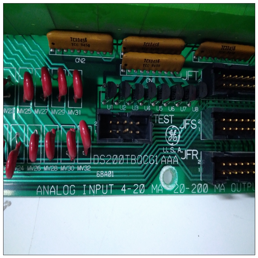
DS200TBQCG1AAA燃机卡件,GE怎么使用
内存映射有三种观点:1)所有通过处理器总线(MC88110总线)查看的资源,2)映射从本地外围总线查看车载/非车载资源(MC68040兼容总线),以及3)车载资源映射为由VMEbus主机查看(VMEbus内存映射)。处理器总线内存映射应小心,因为所有三个地图都是可编程的。它是建议从处理器总线直接映射到本地应使用外围总线。MVME197LE设备的内存映射如下所示桌子。表1-2是从$00000000到$ffffff的整个地图。
")
DS200TBQCG1AAA燃机卡件许多领域的地图是用户可编程的,建议使用如表所示。这是假设处理器和本地外围总线和本地外围总线与VMEbus之间。这个缓存抑制功能可在MC88110中编程。车载输入/输出空间必须标记为缓存禁止,并在其页表中序列化。表1-3进一步定义本地设备的映射。1、该区域可由用户编程。建议的用途是如表所示。DRAM解码器已编程通过ECDM I2CBus接口在DCAM中。这个处理器总线到本地外围总线和本地
外围总线到处理器总线解码器是在总线开关中编程。本地外围设备VMEbus(主)和VMEbus到本地外围总线(从)解码器在VMEchip2中编程。2、尺寸为近似值。3.缓存抑制取决于映射区域中的设备。4、该区域未解码。如果访问这些位置并且本地外围总线计时器启用,循环超时并由TEA信号终止。该区域可通过总线开关进行用户编程。默认大小为4MB。有关寄存器位的完整描述,请参阅特定芯片的适当数据表。对于更详细的内存映射请参阅详细的MVME197LE中的外围设备内存映射,MVME197DP和MVME197SP单板计算机程序员参考指南。2.Address是指向设备的物理地址。它是从MC88110转换总线开关后设备的地址。写入VMEchip2中的LCSR必须为32位。8位或16位的LCSR写入以TEA信号终止。对GCSR的写入可以是8位、16位或32位。读取到LCSR和GCSR可以是8、16或32位。4、该区域不返回确认信号。如果处理器总线超时计时器已启用,访问时间输出并由TEA信号终止。5、尺寸为近似值。6.82596CA的端口命令必须写成两个16位写入:第一个上字,第二个下字。7.DROM(启动ROM)在本地外围总线重置。DROM显示为0,直到DR0位在PCCchip2中被清除。DR0位为位于地址0位D15。DROM必须是在0时禁用,然后访问DRAM。
There are three points of view for the memory maps: 1) the mapping of all
resources as viewed by the Processor Bus (MC88110 bus), 2) the mapping of
onboard/off-board resources as viewed from the Local Peripheral Bus
(MC68040 compatible bus), and 3) the mapping of onboard resources as
viewed by VMEbus Masters (VMEbus memory map).
Processor Bus Memory Map
Care should be taken, since all three maps are programmable. It is
recommended that direct mapping from the Processor Bus to the Local
Peripheral Bus be used.The memory maps of MVME197LE devices are provided in the following
tables. Table 1-2 is the entire map from $00000000 to $FFFFFFFF. Many areas
of the map are user-programmable, and suggested uses are shown in the table.
This is assuming no address translation is used between the processor and
local peripheral bus and between the local peripheral bus and VMEbus. The
cache inhibit function is programmable in the MC88110. The onboard I/O
space must be marked cache inhibit and serialized in its page table. Table 1-3
further defines the map for the local devices.1. This area is user-programmable. The suggested use is
shown in the table. The DRAM decoder is programmed
in the DCAM through the ECDM I2CBus interface. The
Processor Bus to Local Peripheral Bus and the Local
Peripheral Bus to Processor Bus decoders are
programmed in the BusSwitch. The Local Peripheral to
VMEbus (master) and VMEbus to Local Peripheral Bus
(slave) decoders are programmed in the VMEchip2.
2. Size is approximate.
3. Cache inhibit depends on devices in area mapped.
4. This area is not decoded. If these locations are accessed
and the local peripheral bus timer is enabled, the cycle
times out and is terminated by a TEA signal.
5. This area is user programmable via the BusSwitch.
Default size is 4 megabytes.For a complete description of the register bits, refer to
the appropriate data sheet for the specific chip. For a
more detailed memory map refer to the detailed
peripheral device memory maps in the MVME197LE,
MVME197DP, and MVME197SP Single Board
Computers Programmer’s Reference Guide.
2. Address is the physical address going to the device. It is
after the BusSwitch translation from the MC88110
address to the device seen address.Writes to the LCSR in the VMEchip2 must be 32 bits.
LCSR writes of 8 or 16 bits terminate with a TEA signal.
Writes to the GCSR may be 8, 16, or 32 bits. Reads to the
LCSR and GCSR may be 8, 16, or 32 bits.
4. This area does not return an acknowledge signal. If the
processor bus timeout timer is enabled, the access times
out and is terminated by a TEA signal.
5. Size is approximate.
6. Port commands to the 82596CA must be written as two
16-bit writes: upper word first and lower word second.
7. DROM (BOOT ROM) appears at $0 following a local
peripheral bus reset. The DROM appears at 0 until the
DR0 bit is cleared in the PCCchip2. The DR0 bit is
located at address 0 bit D15. The DROM must be
disabled at 0 before the DRAM is accessed.

