


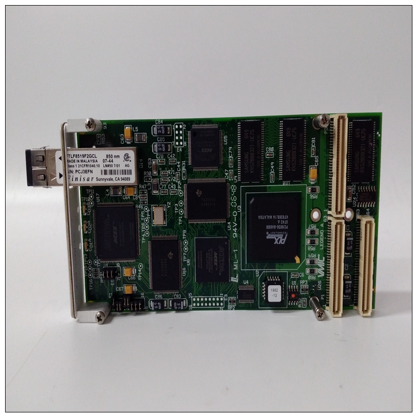
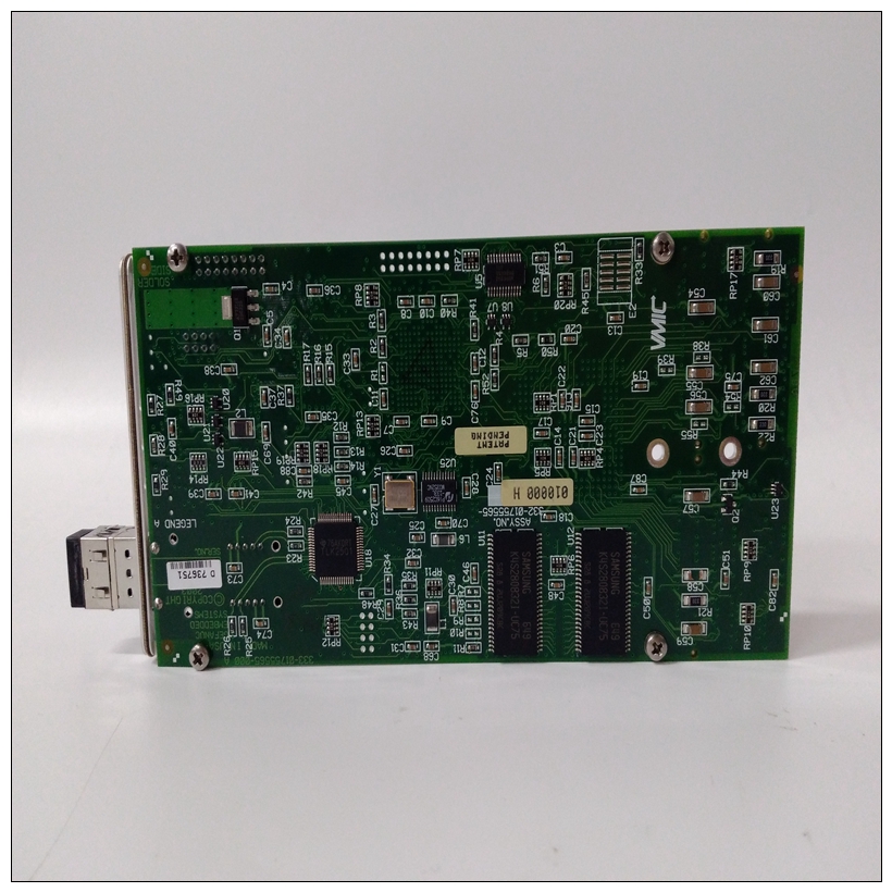
VMIPMC-5565燃机卡件,GE参数说明
当该位为1(高)时,它指示调试器使用用于其工作页的本地静态RAM(即变量、堆栈、向量表等)。当拆下跳线时,该位将为高位。位#1(GPI1)3-4当该位为1(高)时,它指示调试器使用ROM中的默认设置/操作参数与NVRAM中的用户设置/操作参数。这是一样的同时按下重置和中止开关时间如果用户设置为损坏或不符合健全性检查。参考ENVROM默认值的命令(附录A)。此位将拆下跳线时为高。
")
VMIPMC-5565燃机卡件可选SRAM备用电源选择头J6标头J6是一个可选标头,用于选择SRAM备份MVME187上的电源(如果有可选电池)。(SRAM的备用电池可选,但仅作为工厂建造,仅根据特殊要求。)
如果您的系统配备了可选电池备用,不要从J6上拆下跳线。这将禁用SRAM。如果您的电路板包含可选的收割台J6,但可选电池已拆下,跳线必须安装在针脚1和3以及针脚2和4之间工厂配置如表3-5所示。串行端口4时钟配置选择头J7和J8串行端口4可以配置为使用TRXC4和RTXC4信号线。MVME187上的头J7和J8配置串行端口4以驱动或分别接收TRXC4和RTXC4(见表3-6)。
❏ 出厂配置将端口4设置为接收两个信号。
❏ 替代配置将端口4设置为驱动两个信号时钟线的其余配置完成使用上的串行端口4时钟配置选择标头MVME712M过渡模块。参考MVME712M过渡模块和P2适配器板用户手册该标头的配置。
When this bit is a one (high), it instructs the debugger to use
local Static RAM for its work page (i.e., variables, stack, vector
tables, etc.). This bit will be high when jumper is removed.
Bit #1 (GPI1) 3-4 When this bit is a one (high), it instructs the debugger to use
the default setup/operation parameters in ROM versus the
user setup/operation parameters in NVRAM. This is the same
as depressing the RESET and ABORT switches at the same
time. This feature can be used in the event the user setup is
corrupted or does not meet a sanity check. Refer to the ENV
command (Appendix A) for the ROM defaults. This bit will be
high when jumper is removed.Optional SRAM Backup Power Source Select Header J6
Header J6 is an optional header used to select the SRAM backup
power source on the MVME187, if the optional battery is present.
(The battery backup for SRAM is optionally available, but only as a
factory build and only by special request.)
!
Caution
If your system is equipped with the optional battery
backup, do not remove the jumpers from J6. This will
disable the SRAM. If your board contains optional
header J6, but the optional battery is removed, jumpers
must be installed between pins 1 and 3 and pins 2 and 4
for the factory configuration as shown in Table 3-5.
Serial Port 4 Clock Configuration Select Headers J7 and J8
Serial port 4 can be configured to use clock signals provided by the
TRXC4 and RTXC4 signal lines.
Headers J7 and J8 on the MVME187 configure serial port 4 to drive
or receive TRXC4 and RTXC4, respectively (see Table 3-6).
❏ Factory configuration sets port 4 to receive both signals.
❏ The alternative configuration sets port 4 to drive both signals
The remaining configuration of the clock lines is accomplished
using the Serial Port 4 Clock Configuration Select header on the
MVME712M transition module. Refer to the MVME712M
Transition Module and P2 Adapter Board User's Manual for
configuration of that header.

