


KLA Tencor 820-23075-000接口连接器板 PDF资料
1.产 品 资 料 介 绍:
中文资料:
KLA Tencor 820-23075-000 接口连接器板是一种用于半导体检测设备内部模块连接的电子组件,主要应用于高端晶圆检测设备,特别是电子束(E-beam)检测平台。以下是其详细的产品应用领域说明:
产品类型
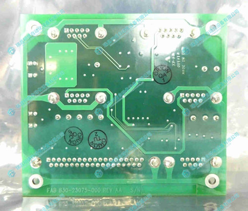
部件号:820-23075-000
名称:接口连接器板(Interface Connector Board)
制造商:KLA Tencor
产品应用领域
1. 电子束晶圆缺陷检测系统
被广泛应用于 KLA Tencor eS 系列(如 eS31)电子束晶圆检测设备中。
这些设备利用电子束扫描实现亚微米级别的晶圆表面缺陷检测,适用于先进制程节点(如 7nm、5nm、3nm)的制造流程。
2. 设备内部通信与连接
该板卡作为系统内部各模块(图像采集、电源分配、处理器、控制器等)之间的信号和电源连接中枢。
具备高密度接线和多接口支持,确保高速数据和控制信号稳定传输。
3. 高精度检测环境中的协同控制
在极为复杂且高精度的检测平台中,接口连接器板确保各控制模块之间的精确同步,有助于保持图像分辨率、扫描速度和数据处理的协调一致性。
4. 可靠性与抗干扰设计
设计上注重电气隔离和抗电磁干扰性能,确保在高速、高频运行环境中仍保持系统可靠性。
典型使用环境
半导体晶圆制造工厂(如台积电、英特尔、三星)
高端IC设计与流片测试中心
晶圆制造过程中的先进制程监测站
英文资料:
The KLA Tencor 820-23075-000 interface connector board is an electronic component used for internal module connections in semiconductor inspection equipment, mainly applied in high-end wafer inspection equipment, especially in electron beam (E-beam) inspection platforms. The following is a detailed explanation of its product application areas:
product type
Part number: 820-23075-000
Name: Interface Connector Board
Manufacturer: KLA Tencor
Product application areas
1. Electron beam wafer defect detection system
Widely used in KLA Tencor eS series (such as eS31) electron beam wafer inspection equipment.
These devices utilize electron beam scanning to achieve sub micron level wafer surface defect detection, suitable for manufacturing processes at advanced process nodes such as 7nm, 5nm, 3nm.
2. Internal communication and connection of equipment
This board serves as the signal and power connection hub between various modules within the system (image acquisition, power distribution, processor, controller, etc.).
Equipped with high-density wiring and multi interface support, ensuring stable transmission of high-speed data and control signals.
3. Collaborative control in high-precision detection environments
In extremely complex and high-precision detection platforms, the interface connector board ensures precise synchronization between various control modules, helping to maintain coordinated consistency in image resolution, scanning speed, and data processing.
4. Reliability and anti-interference design
In terms of design, emphasis is placed on electrical isolation and anti electromagnetic interference performance to ensure system reliability even in high-speed and high-frequency operating environments.
Typical usage environment
Semiconductor wafer manufacturing factories (such as TSMC, Intel, Samsung)
High end IC Design and Chip Testing Center
Advanced process monitoring station in wafer manufacturing process
2.产 品 展 示
")
3.其他产品
4.其他英文产品
DS200TCEAG1BNE emergency overspeed board
ASEA DSQC223 Robot Control Board
| 6ES5726-1CB00 | CACR-HR10UB | Asyst 3200-4346-02 |
| 6ES5725-7CF00 | CACR-IR44SFBY8 | ASYST 3200-1045-02 |
| 6ES5725-0BJ00 | CACR-SR10BF1AMB | Asyst 3200-1225-05 |
| 6ES5721-5CB00 | CACR-UP130AABY21 | Asyst 3200-4348-02 |
| 6ES5721-4BF00 | CACR-330-FF1VBDY71 | C2133 ASYST INC 3200-1045-01 3200-1065-01 |
| 6ES5721-0CG30 | CACR-SR20BE | Asyst 3200-1101-02 |
| 6ES5721-0CC00 | CACR-SR15BE13S | Asyst 3200-1251-02 |
本篇文章出自瑞昌明盛自动化设备有限公司官网,转载请附上此链接:http://www.jiangxidcs

