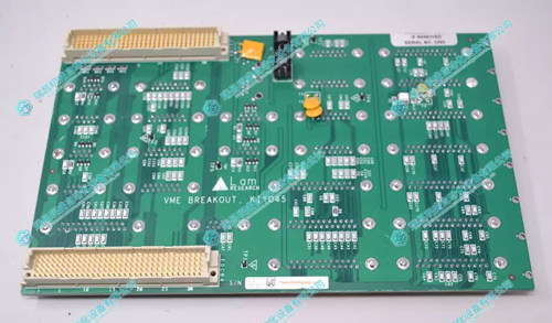
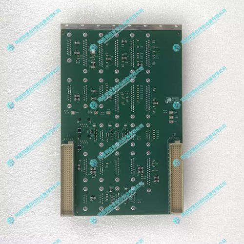
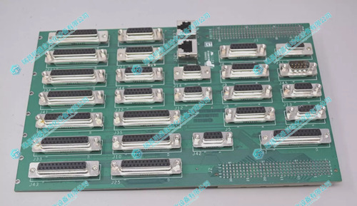
LAM 810-800082-243印刷电路板 PDF资料
1.产 品 资 料 介 绍:
中文资料:
LAM 810-800082-243 印刷电路板(PCB)是由 LAM Research 公司生产的一种高精度、高可靠性的电路板,通常用于半导体制造设备中,特别是在化学气相沉积(CVD)、刻蚀设备等高度复杂的设备中。它作为核心组件之一,承担着信号传输、电源管理和设备控制等多重功能。
主要特性:
高质量材料
该PCB采用高质量的材料,如高频基板和精密金属化技术,以确保在复杂和高要求的环境下提供稳定的性能。多层设计
该印刷电路板通常具有多层结构,确保有足够的信号传输通道,同时减少干扰,优化电气性能。多层设计提高了其承载能力和信号传输的准确性。耐用性与稳定性
采用工业级标准设计,具备较高的抗热、抗干扰和抗机械振动能力。特别适合在半导体制造设备的高温、高湿环境中长期运行。精确信号处理
该电路板负责对各类信号进行精确处理,并且能够通过特定的接口模块与其他控制系统进行无缝通信。高密度封装技术
采用高密度封装(如SMT)和紧凑型布局,优化了电路板的空间利用率,同时提升了电气性能和响应速度。
典型应用:
半导体制造设备
用于刻蚀、薄膜沉积、离子注入等工艺的自动化控制系统。化学气相沉积(CVD)设备
在CVD反应室中用于精确控制气体流量、电流、压力等参数。等离子体清洗设备
用于高精度清洗半导体晶圆表面,确保工艺的高度一致性。自动化测试设备
用于测试和分析半导体芯片的性能,支持数据传输、处理与分析。
英文资料:
The LAM 810-800082-201 interface board module is one of the common key components in semiconductor equipment produced by LAM Research, typically used to support process control and data communication. This type of interface board module is widely used in semiconductor manufacturing equipment, such as etching machines, chemical vapor deposition equipment, etc., to provide stable signal transmission and equipment control.
Main features:
High reliability design
The module has strong anti-interference ability and durability, ensuring stable operation in harsh semiconductor manufacturing environments.
Multi functional interface support
Provide support for multiple communication protocols, including serial interfaces, parallel interfaces, and proprietary communication interfaces, for data transmission and control signals between devices.
Modular structure
Easy to integrate into existing device systems and support quick replacement and maintenance.
High precision and fast response
Through high-performance processors and efficient communication mechanisms, precise control and real-time response of semiconductor processes can be achieved.
Application areas:
Semiconductor etching equipment
Chemical Vapor Deposition (CVD) Equipment
Wafer inspection and measurement equipment
Other industrial equipment that requires high-performance signal transmission
Technical parameters (subject to actual equipment):
Power requirements: Standard industrial voltage input, typically 24V DC or 5V DC.
Working temperature range: Supports industrial grade working environments, typically ranging from 0 ° C to 50 ° C.
Interface types: Multiple input/output ports, specific models support RS-232, RS-485, or Ethernet interfaces, etc.
Data transmission rate: It can support transmission rates of up to several hundred Mbps according to demand.
Precautions for use:
Ensure compatibility between modules and devices, carefully check electrical and mechanical specifications before installation.
Follow the manufacturer's instructions for operation to avoid exceeding the specified electrical parameter range.
Regularly check the connection and status of the module to ensure the normal operation of the interface board.
LAM 810-800082-243 printed circuit board (PCB) is a high-precision and high reliability circuit board produced by LAM Research, commonly used in semiconductor manufacturing equipment, especially in highly complex equipment such as chemical vapor deposition (CVD) and etching equipment. As one of the core components, it undertakes multiple functions such as signal transmission, power management, and device control.
Main features:
High quality materials
This PCB uses high-quality materials such as high-frequency substrates and precision metallization technology to ensure stable performance in complex and demanding environments.
Multi layer design
This printed circuit board typically has a multi-layer structure, ensuring sufficient signal transmission channels while reducing interference and optimizing electrical performance. Multi layer design improves its load-bearing capacity and signal transmission accuracy.
Durability and stability
Designed according to industrial standards, it has high resistance to heat, interference, and mechanical vibration. Especially suitable for long-term operation in high-temperature and high humidity environments of semiconductor manufacturing equipment.
Accurate signal processing
This circuit board is responsible for precise processing of various signals and can seamlessly communicate with other control systems through specific interface modules.
High density packaging technology
By adopting high-density packaging (such as SMT) and compact layout, the space utilization of the circuit board has been optimized, while improving electrical performance and response speed.
Typical applications:
Semiconductor manufacturing equipment
An automated control system for processes such as etching, thin film deposition, and ion implantation.
Chemical Vapor Deposition (CVD) Equipment
Used for precise control of gas flow rate, current, pressure, and other parameters in CVD reaction chambers.
Plasma cleaning equipment
Used for high-precision cleaning of semiconductor wafer surfaces to ensure high consistency of the process.
Automated testing equipment
Used for testing and analyzing the performance of semiconductor chips, supporting data transmission, processing, and analysis.
2.产 品 展 示
3.其他产品
4.其他英文产品
Radisys EPC-3307 processor board
ASEA 57360001-AN circuit board
Radisys ATCA-PP81 controller module
| 6ES5376-1AA21 | CACR-IR-020202F | 6DD2920-0BF0 |
| 6ES5376-0AA21 | 6SC6110-6AA00 | 6ES5451-4UA13 |
| 6ES5375-1LA71 | CACR-HR02BAB12 | 6DD2920-0BE0 |
| 6ES5375-1LA21 | 6SC9811-4CH00 | 6ES5450-8MD11 |
| 6ES5375-0LD31 | CACR-HR20BBC | 6DD2920-0BC0 |
| 6ES5375-0LC41 | 6SC6506-0AA02 | 6ES5444-3AA11 |
| 6ES5375-0LC31 | CACR-IR10SB | 6DD2920-0BA0 |
| 6ES5375-0LB11 | 6SC6111-5DA00 | 6ES5440-5AA11 |
| 6ES5375-0LA15 | 6SC6500-0NA44 | 6ES5434-7LA12 |


